
ELEC Final Review
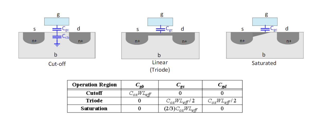
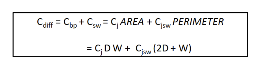
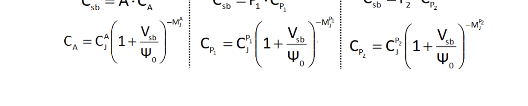
MOS capacitors
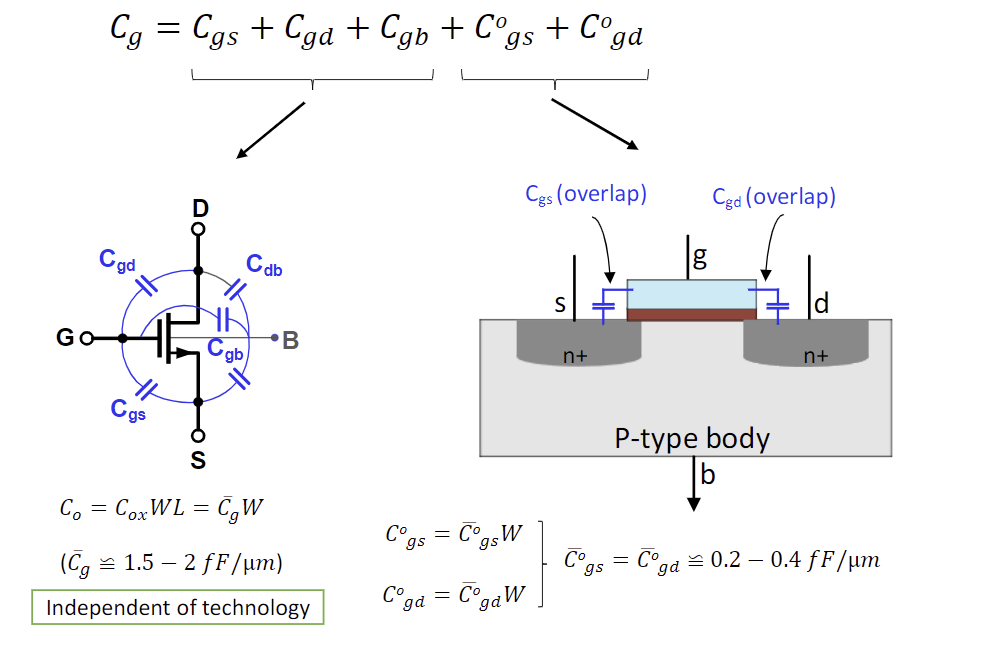
No include the overlap
Combinational Logic
Logical Effort related
Formula for CL , load capacitance
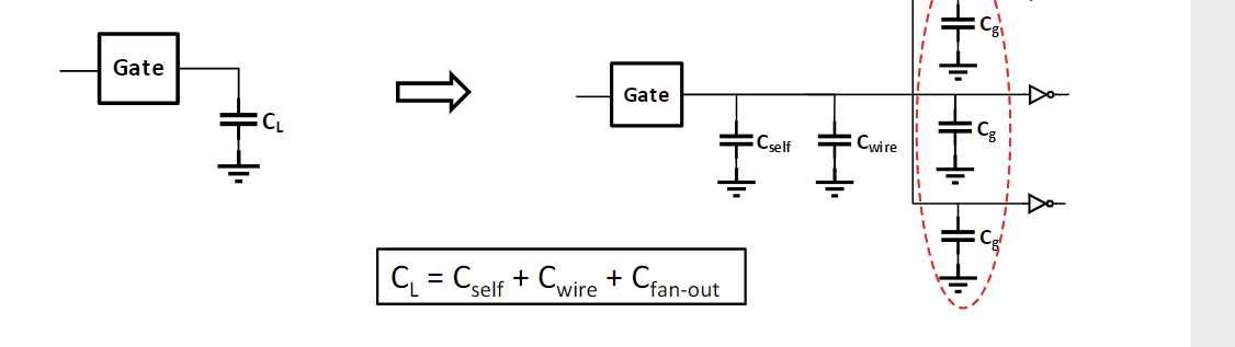
Find the C fanout
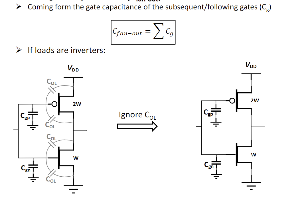
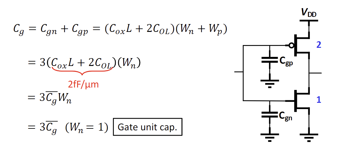
Definition of Cg and Cg bar
Find C wire

Find C self
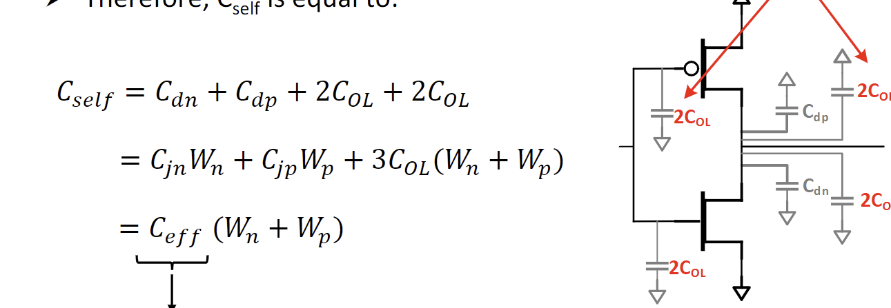
C self for complex gates
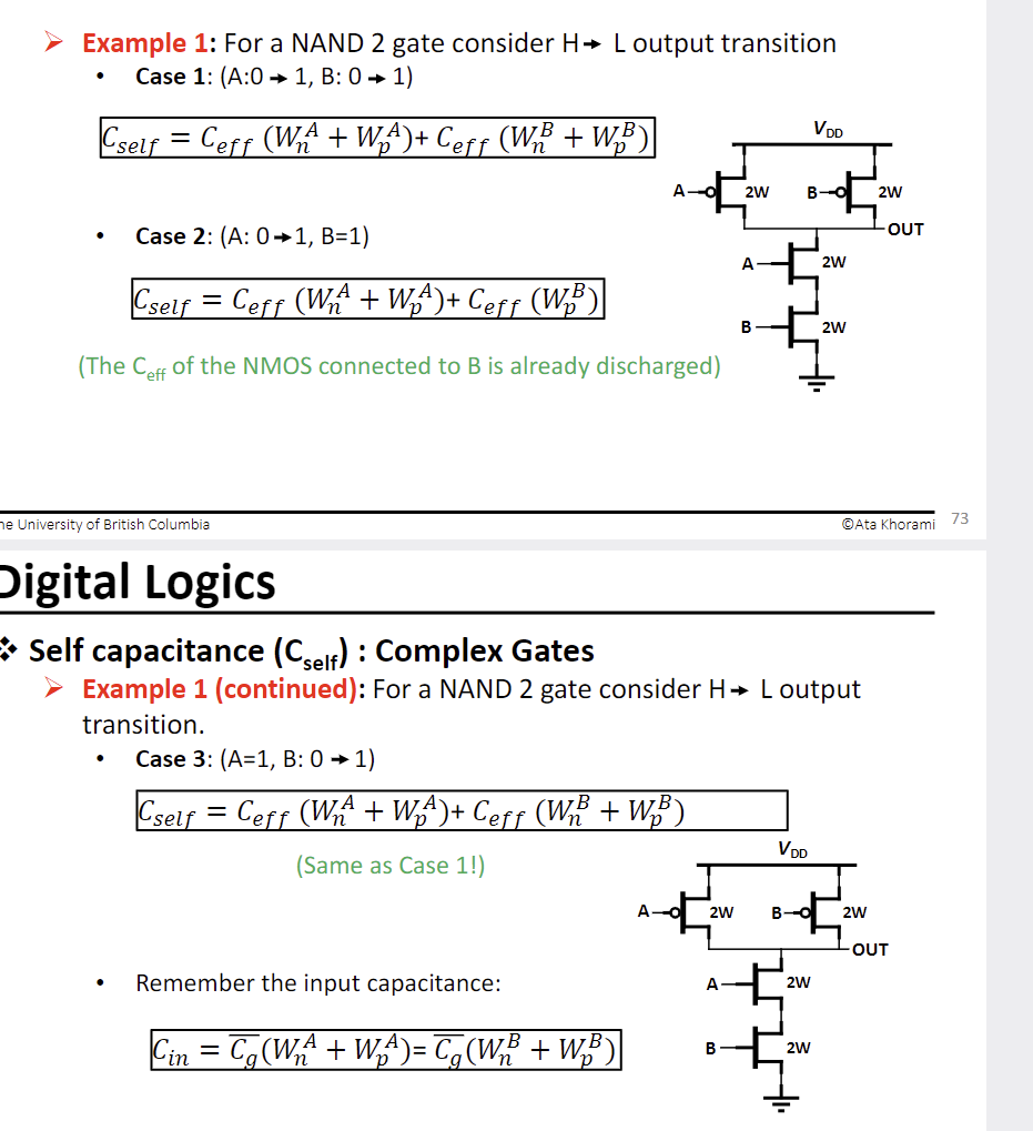
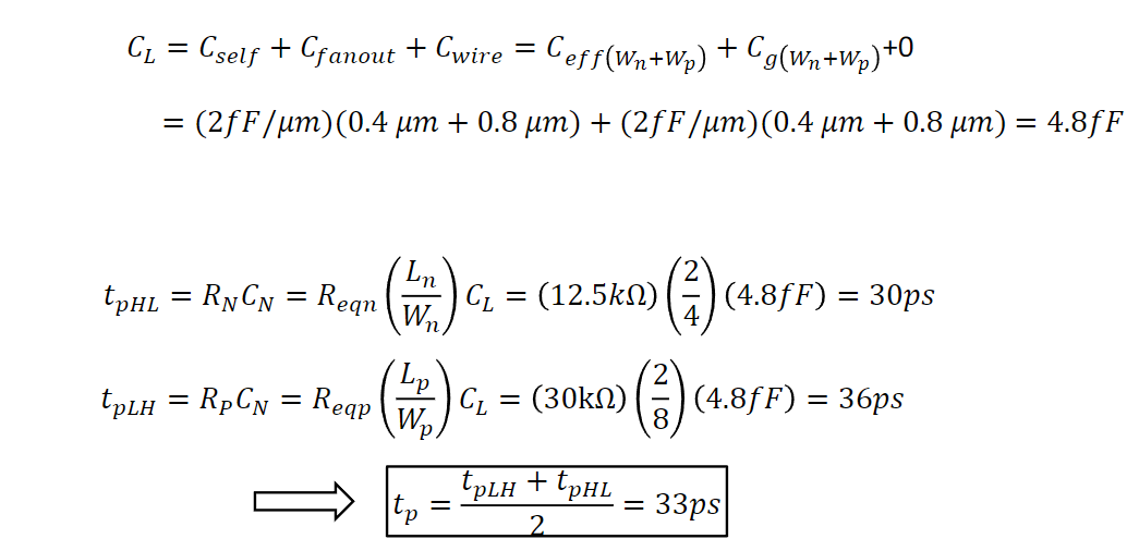
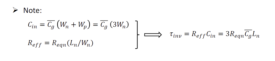
Find Cin and tao
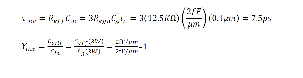
Find gramma
Find delay

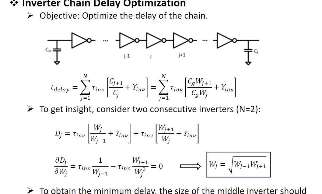
Derivation of the relation of the size of the inverter chain
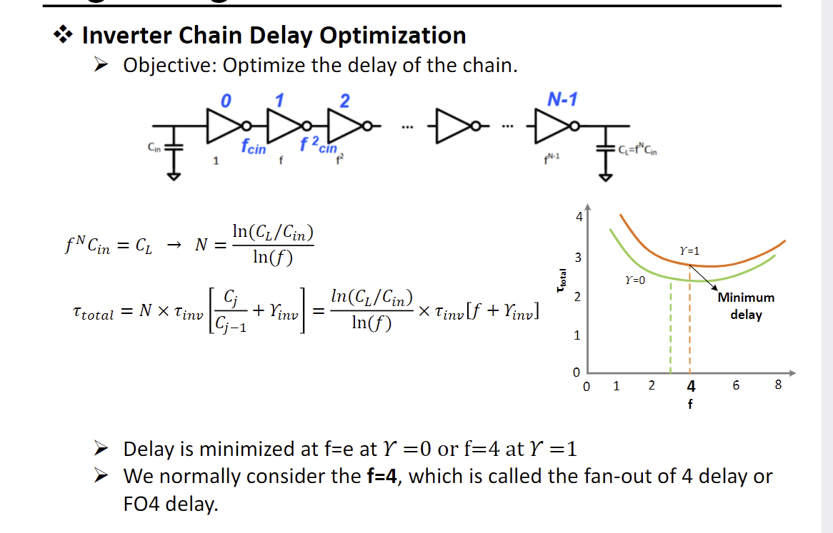
How to find the N for the interter chain
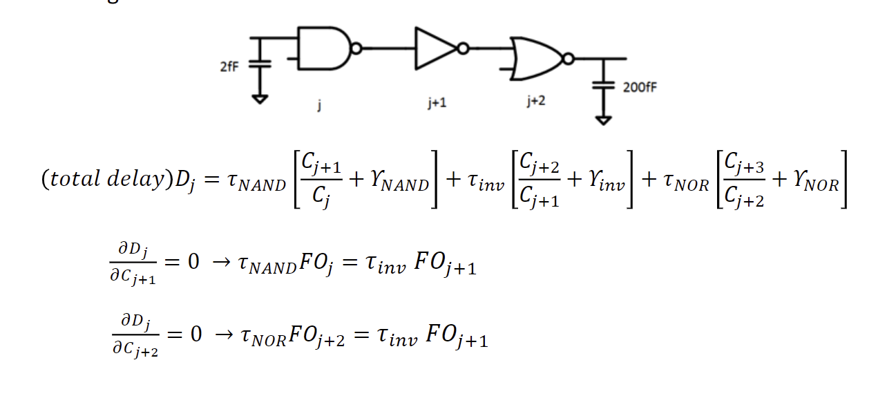
For complex gate, we need to use logical effort
Definition

So we find the delay of complex gate chain by
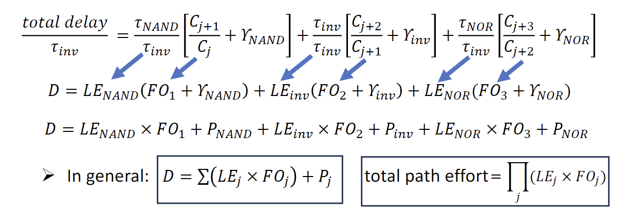
Simplify with logical effort and definition of path effort
P is Parasitic Delay which is LE * gramma
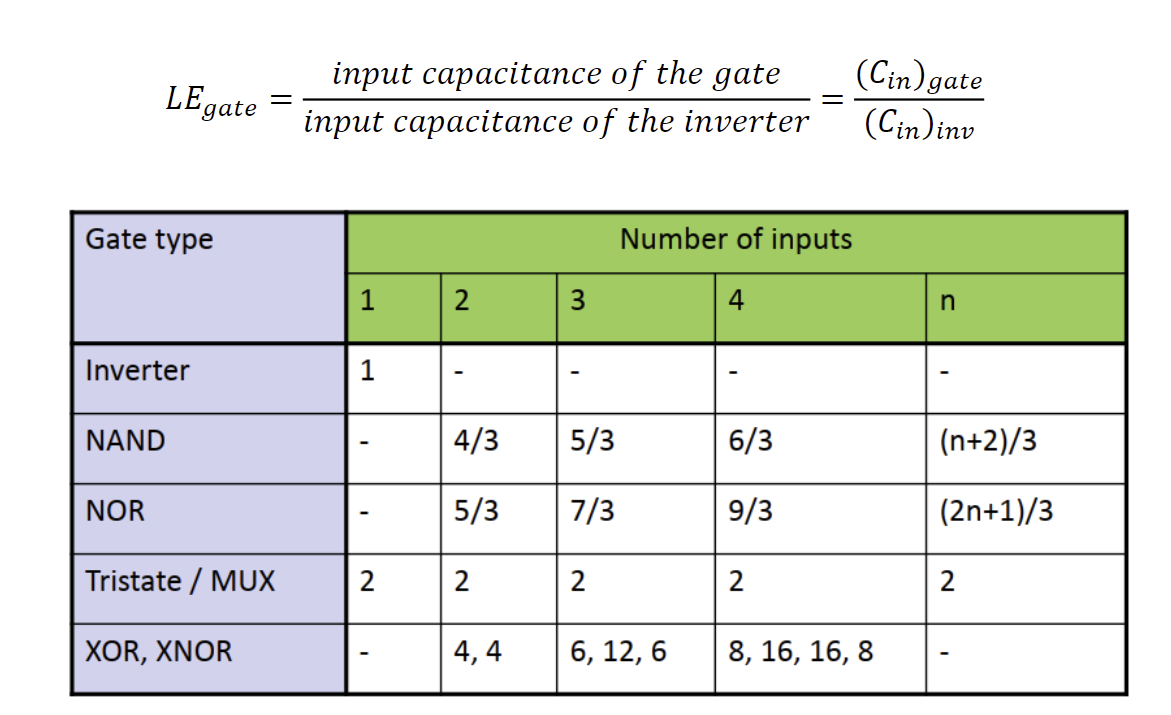
Common logical gate LE
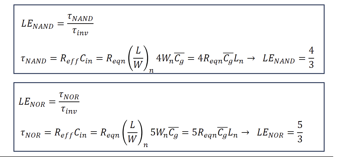
How to find LE your self
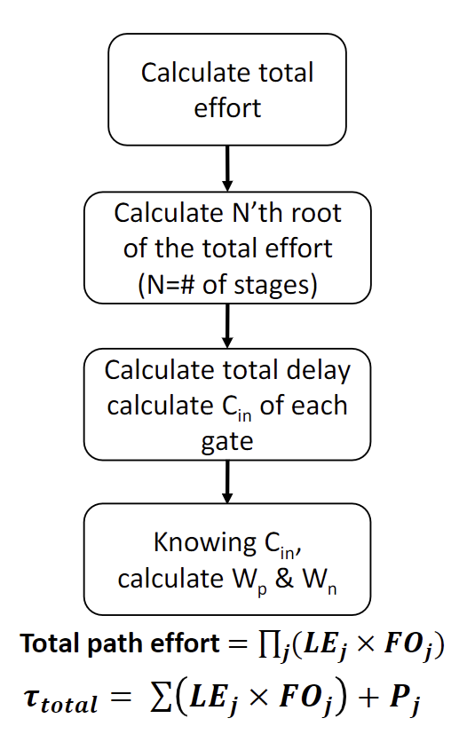
Flow to optimize the delay of logical chain
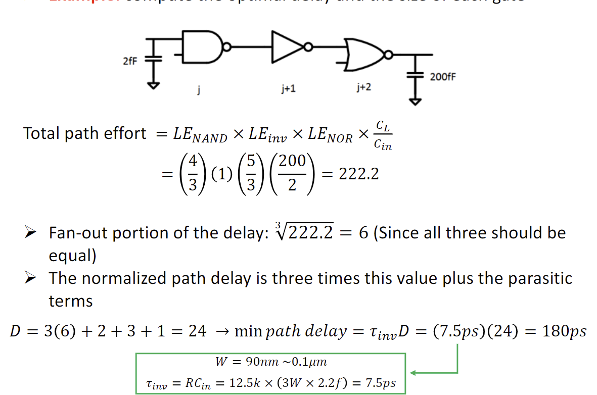
One example
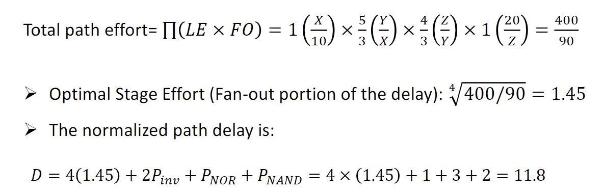
Find totoal path effort -> use path effort to find LE for LE x FO for each stage
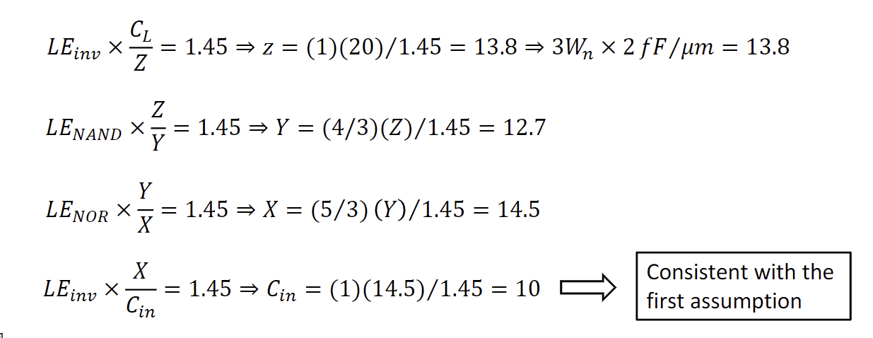
Find intermidiate C for every stage, and use that to find Wn, which is size of each stage
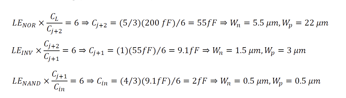
How to get from cap to size ???? use Cin and Cg_bar and size to find the size

Another example
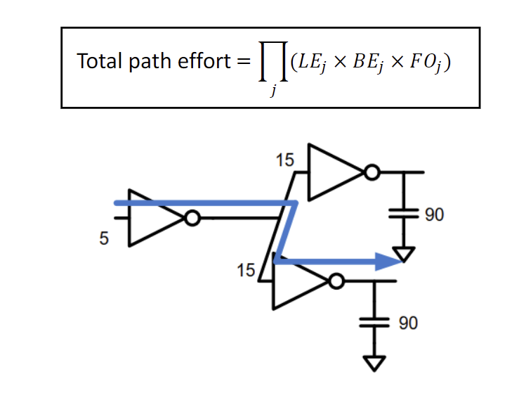
Branch effort
Pseudo-NMOS Logic
We don’t want PMOS in our circuit because PMOS is limiting factor of the mobility
so we have a circuit
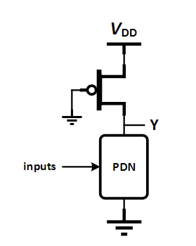
More examples
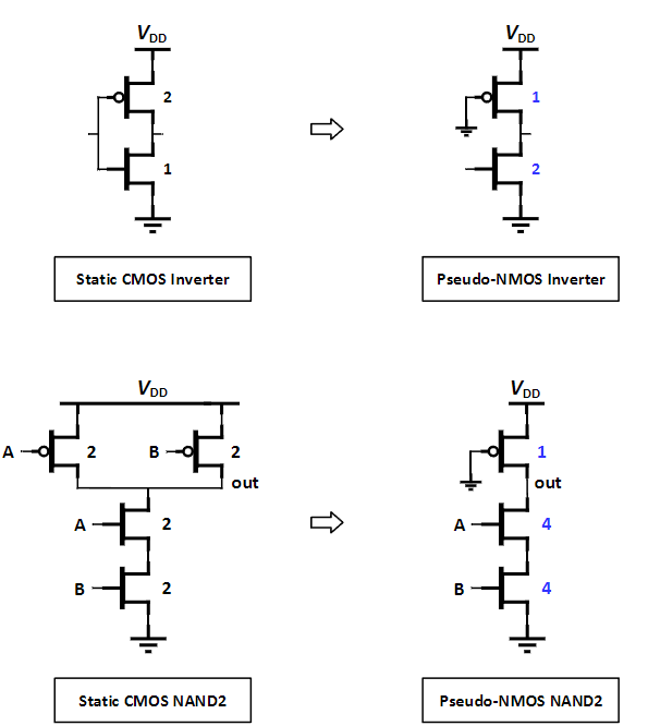
When NMOS is OFF, PMOS pull the outputs to VDD
When NMOS is ON, they fight as PMOS and NMOS become a resistor.
And we need to size NMOS and PMOS to deliver correct
Derviation of
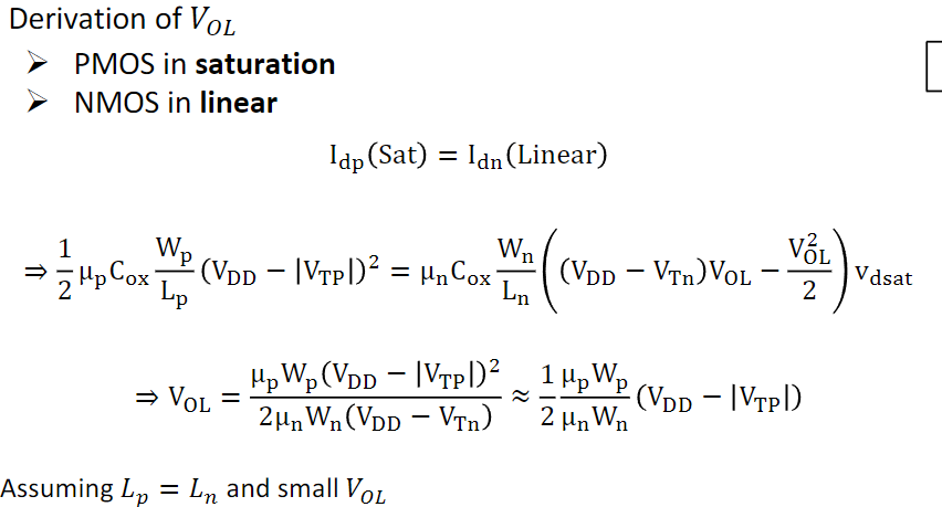
As you can see, we increase increase. We find based on the designed .
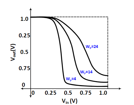
Some example sizing
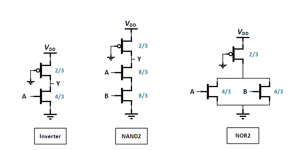
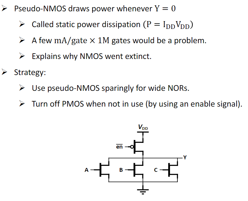
For the power useage ??
The benefits of Pseudo-NMOS logic and drawbacks
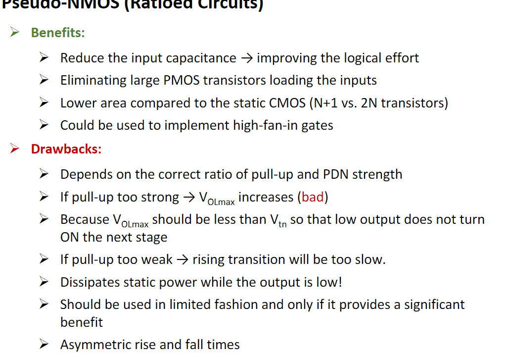
slow rise time
more static power
Dynamic logic
In static circuit, at every point in time, the outputs is connect to either GND or VDD via a lower resistance path.
- Fan-in of N requires 2N devices
Dynamic circuit rely on the temporary storage of singal value on the capacitracne of high impedancce nodes.
- Requires only N+2 transistorr
- Takes a sequence of pre-charge and conditional evalutaion phase to realize logic functions
Dynamic circuit use two step:
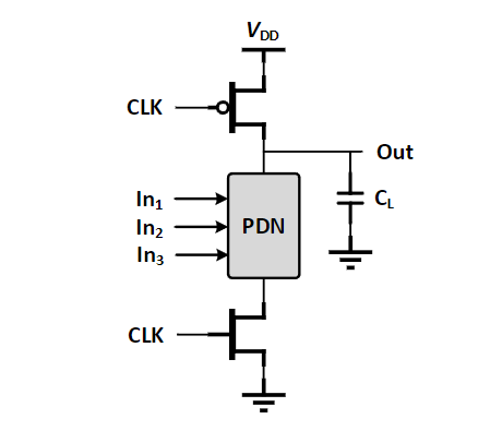
- First precharge the output node to 1
- If pull down is one then output to 0, if pull down is off then output 1
But if pull down is on during precharge, short circuit
Solution
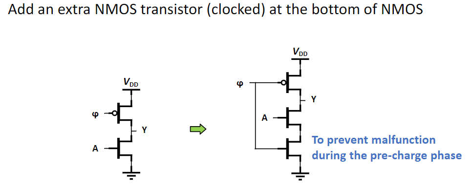
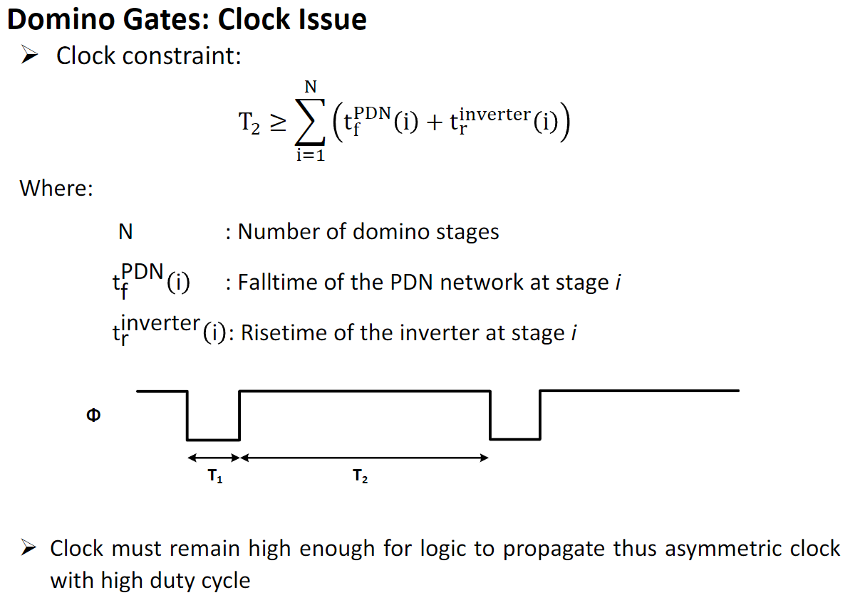
Usually connect this with a clock
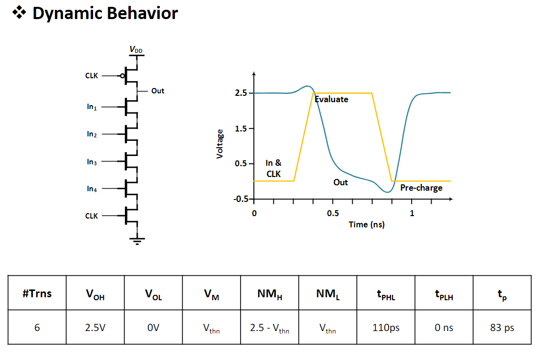
Dynamic behavior
Gate Parameters are Time Independent
- Output voltage drops is strongly depended on the the input voltage and the available evaluation time.
- Noise needed to correupt the signal has to be larger if the evalution time is short
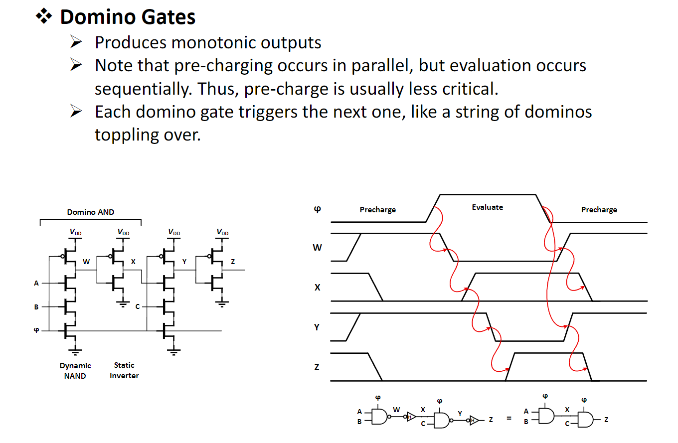
Dynamic gates require “monotonically rising” inputs during evaluation.
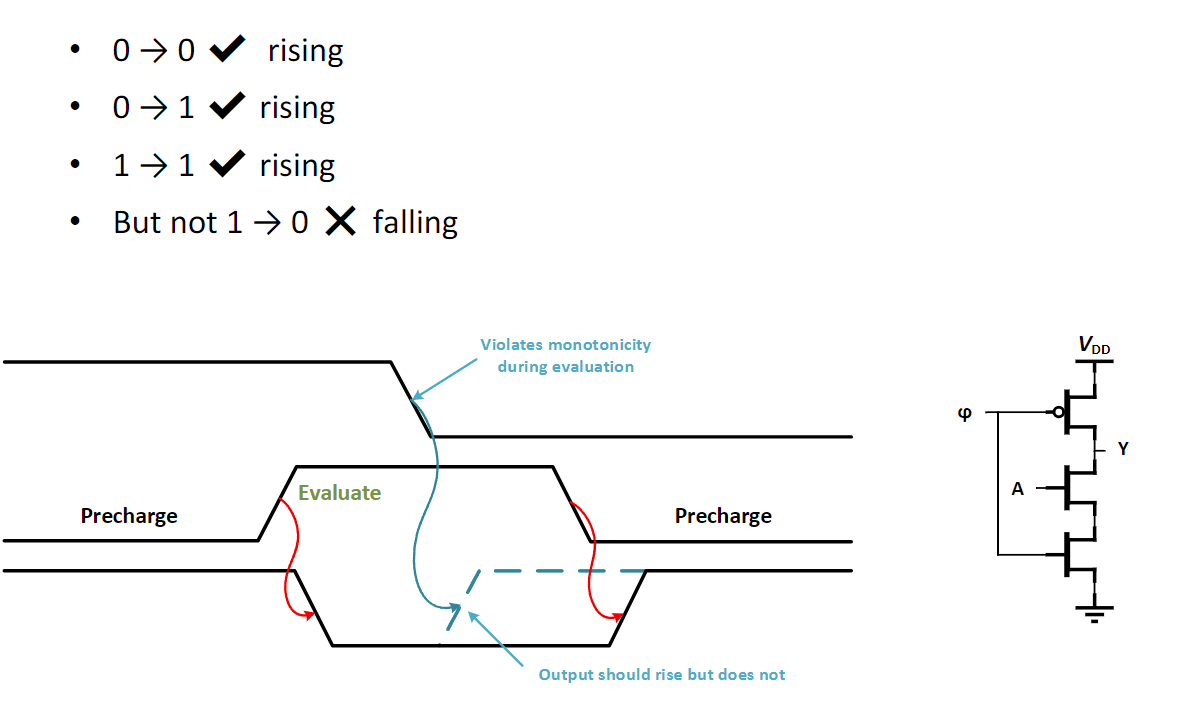
Dynamic gates produce monotonically falling outputs during evaluation while the inputs of the dynamic logic should be monotonically rising because volrtage drops during high and when it 1 -> 0, the voltage level drops and nevre recover
So it is illegal for one dynamic gate to drive another gate
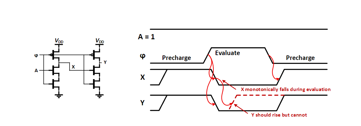
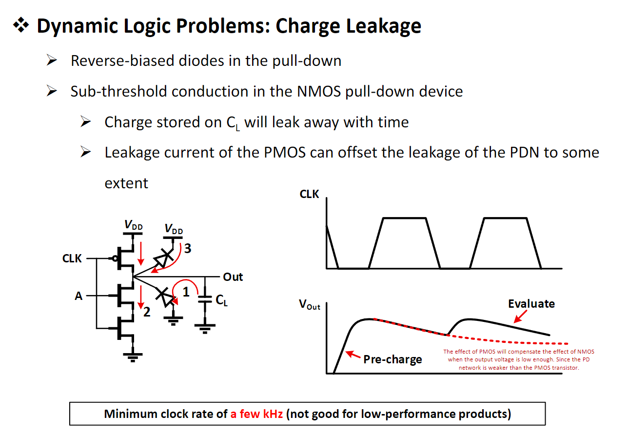
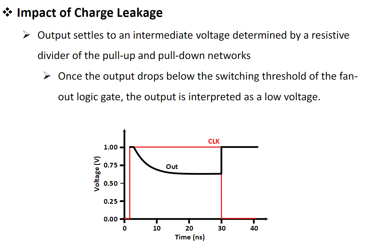
During the transistion, the voltage of Y leaks
Two solution for this:
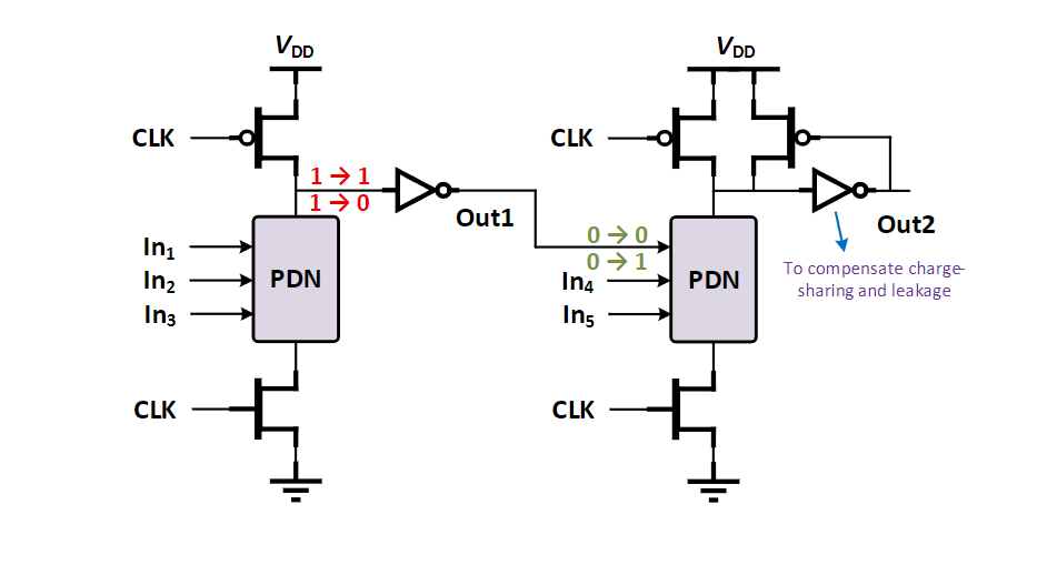
- Place inverter
- One PDN (Pull down), one PUN (Pull up)
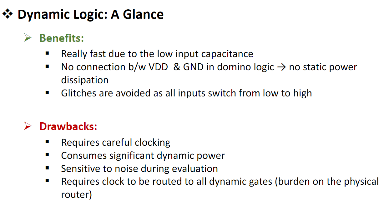
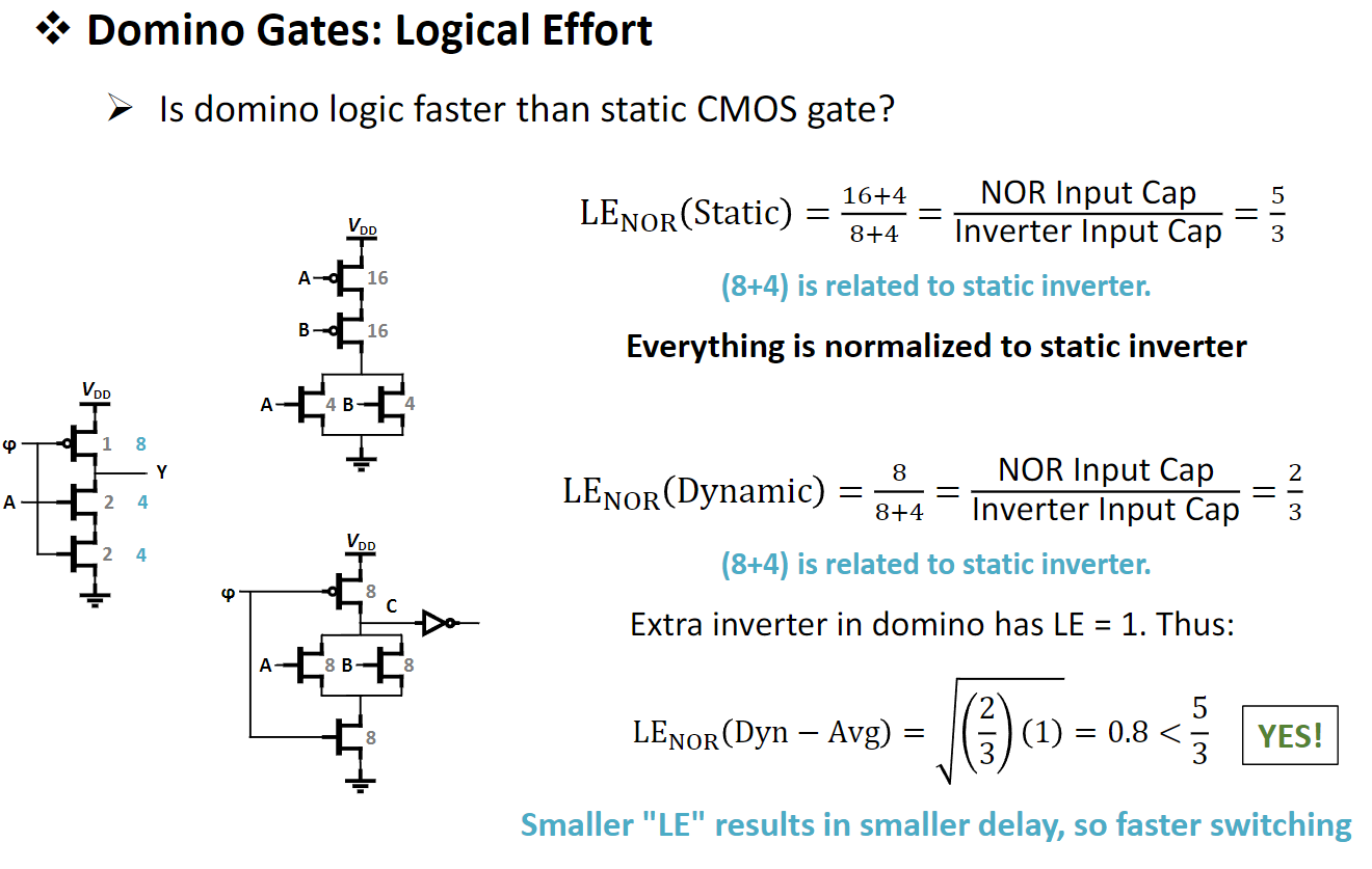
Domino gate
The combination of dynamic/static pair is called domino gate
Logical Effor
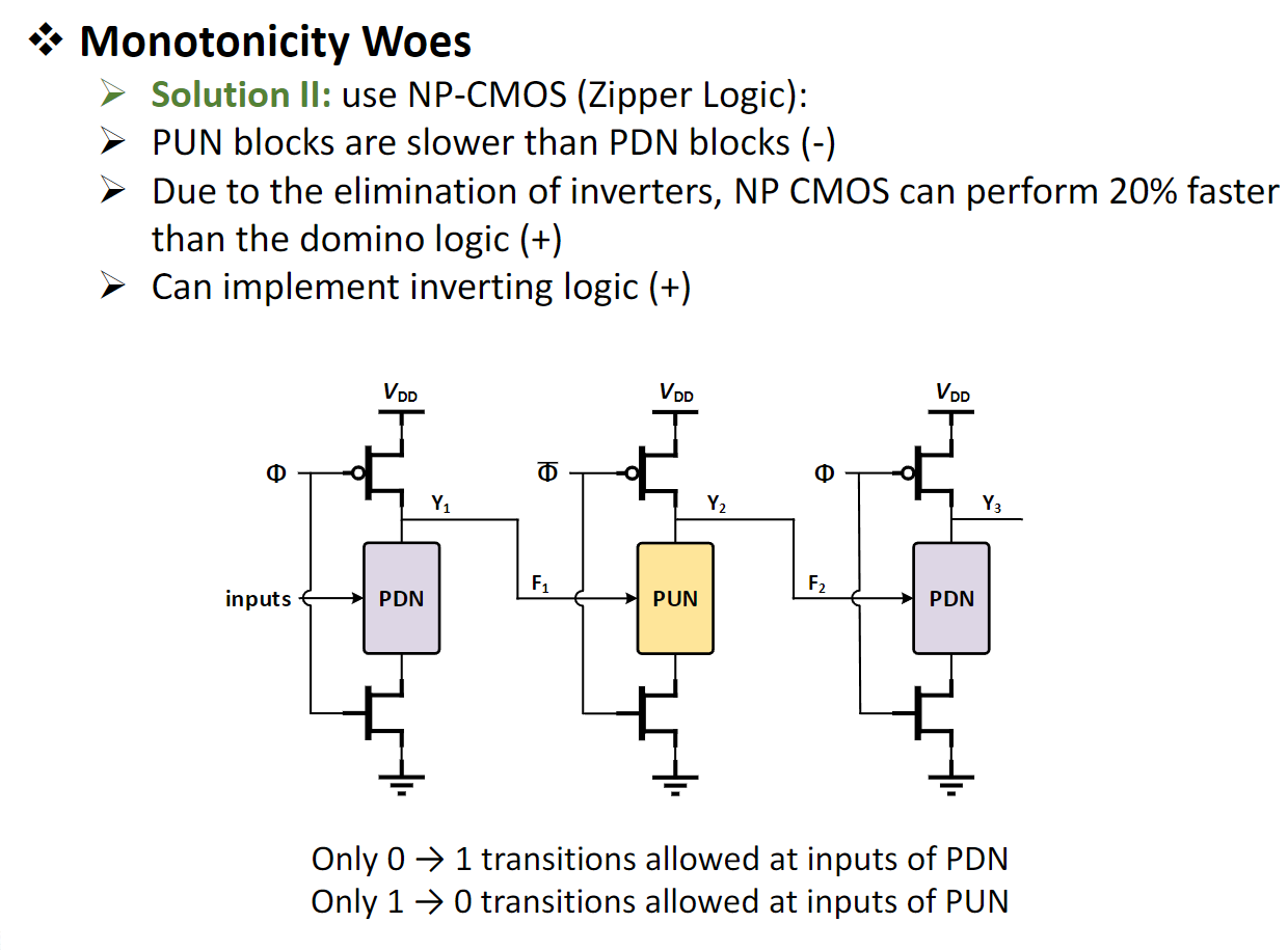
Zipper Logic
The second solution is called Zipepr logic
Dynamic Logic Problems
- Charge Sharing
- Charge Leakage
- Feed Through
- Noise Sensitivity
- CAN tools does not support them very well
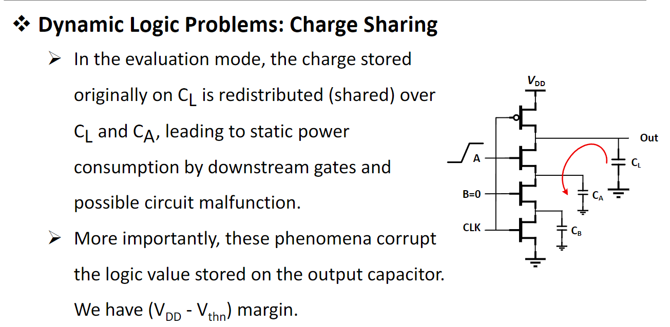
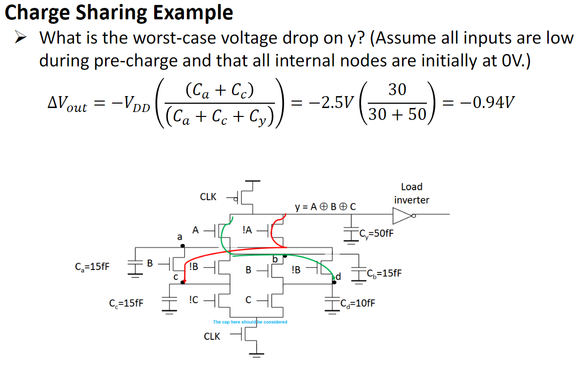
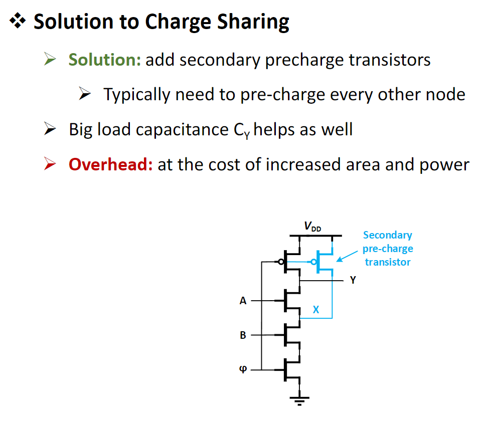
Charge Sharing
output cap charge shared by other node capacitance
charge CA to Vdd - Vthn
corrupt the output logic
worse case, only charged but during eval, and all other node cap are on.
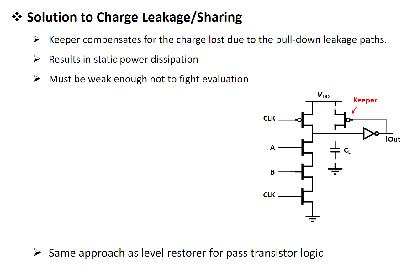
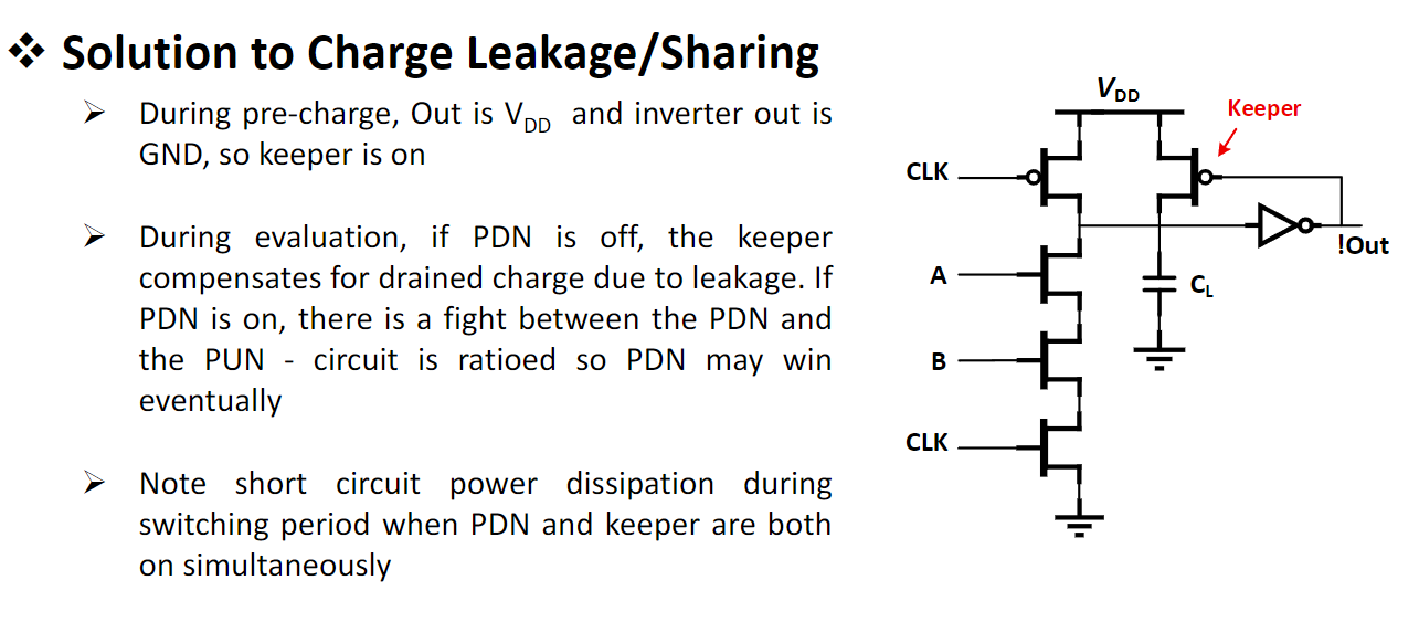
Charge Leakage
Clock Feed-through
A special case of capacitive coupling between the clock input of the pre-charge transistor and the dynamic output node
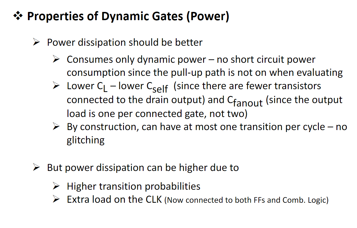
Power
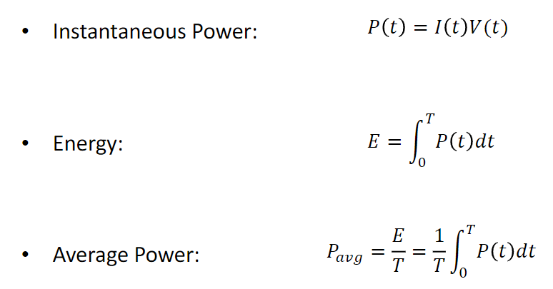
Energy Instantaneous power I x V
Energy intergation of Power
Average power E/T
Dynamic powerL when gate switches
- Charging and discharging
- short circuit power during switching
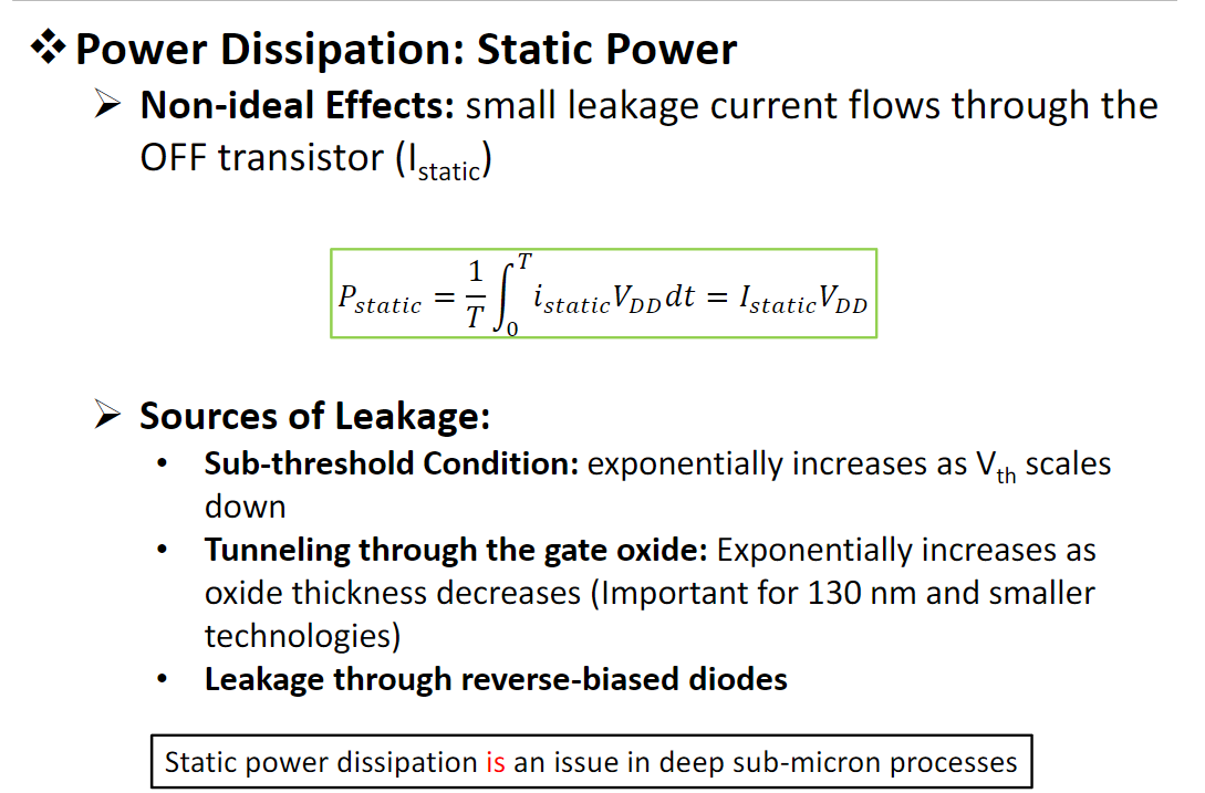
Static power
- subthreshold and junction leakages
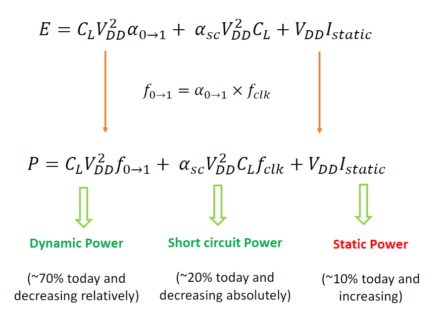
Main Dynamic Power
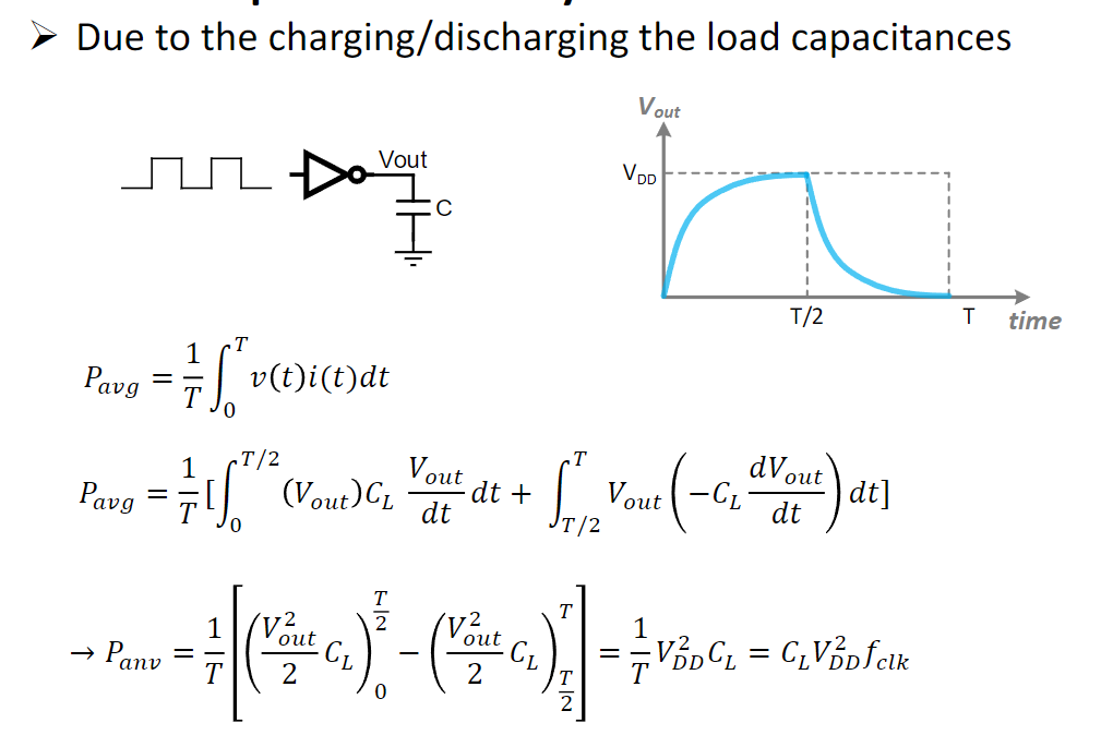
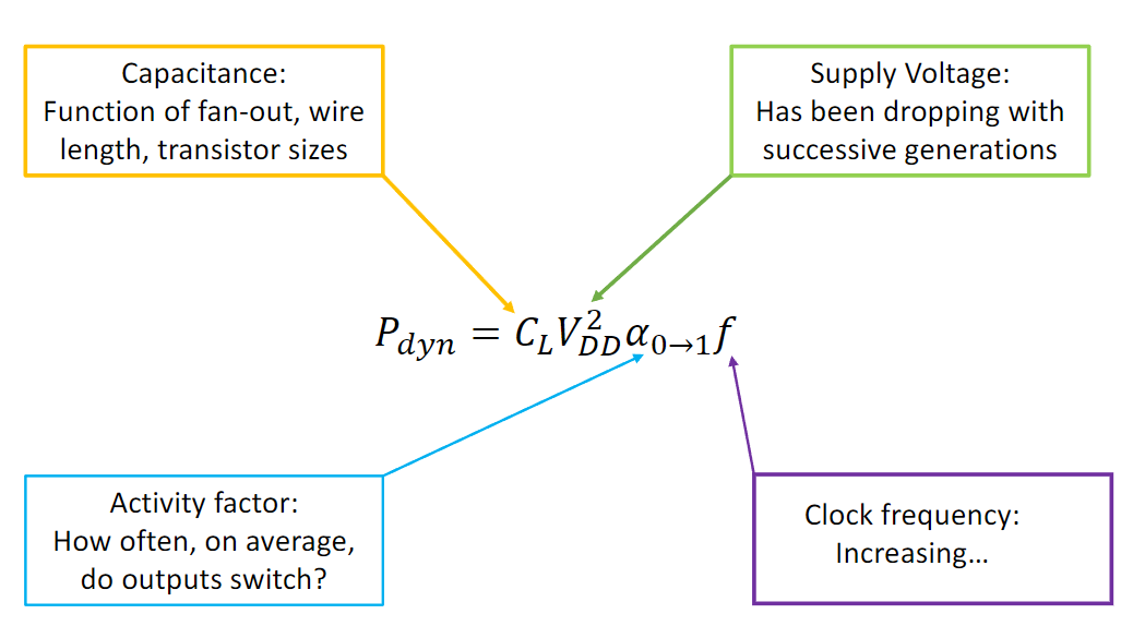
To lower the dynamic power
- Reduce the factor
- smaller capacitance
- smaller trnasistors
- shorter wires
- Lower V
- lower f
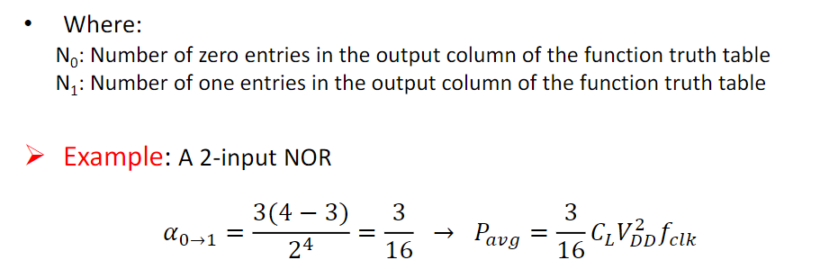
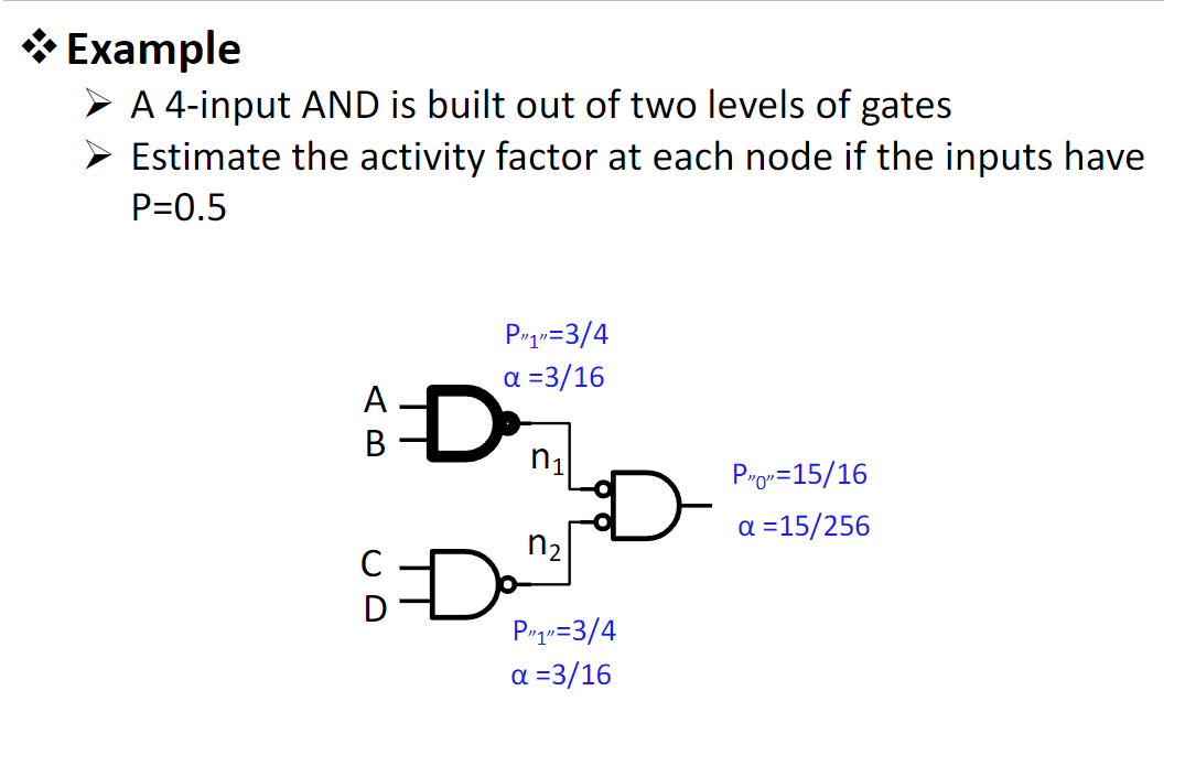
Activity Factor
Probability that output is “zero” in one cycle and will be “one” in the next cycle

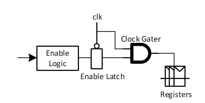
Clock gating
Turn off the clock to registers in unused block
save clock activity
eliminates all switching acivity in the block
Capacitance
- Gate capacitance
- fewer stages of logic
- smaller gate size
- Wire capacitance
- Good floorplanning to keep blockes close to each others
- Drive long wires with inverter of buffer rather than complex gates
Dynamic Power
Run each block at the lowest possible voltage and frequency that meets performance requirements
Voltage domains
- provide separate supplies to different blocks
- level converter required when corssing from low Vdd to high Vdd domains
Dynamic voltage scaling
Adject Vdd and frequency according to workload
Larger V -> Faster f -> higher power
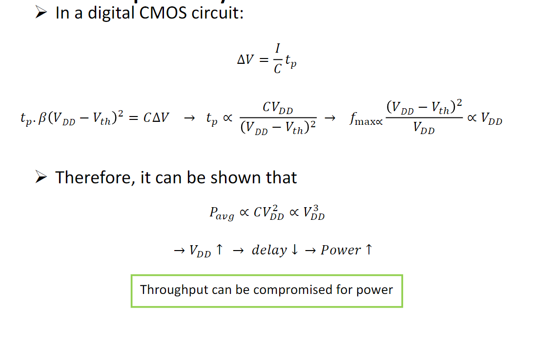
PDP and EDP ??
Power-Delay-Product
- PDP is the average energy consumed per switching
- Lower power design could simply be a slower design
- For a given structure the PDP may be made arbitrary low by reducing the supply voltage that comes at the expense of performance
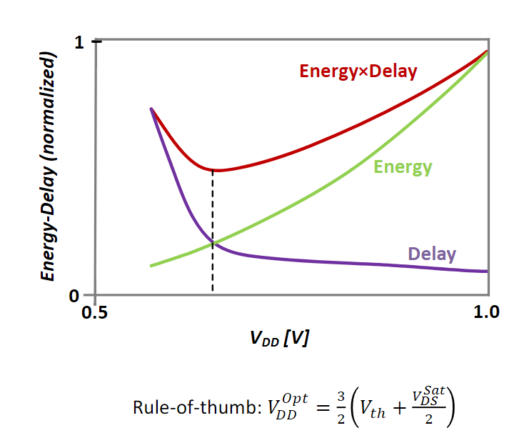
Energy-Delay-Product(EDP)
- EDP is the average energy consumed multiplied by the required computation time
- Takes into account that one can trade increased delay for lower energy/operation (e.g. via supply voltage scaling that increases delay, but decreases energy consumption)
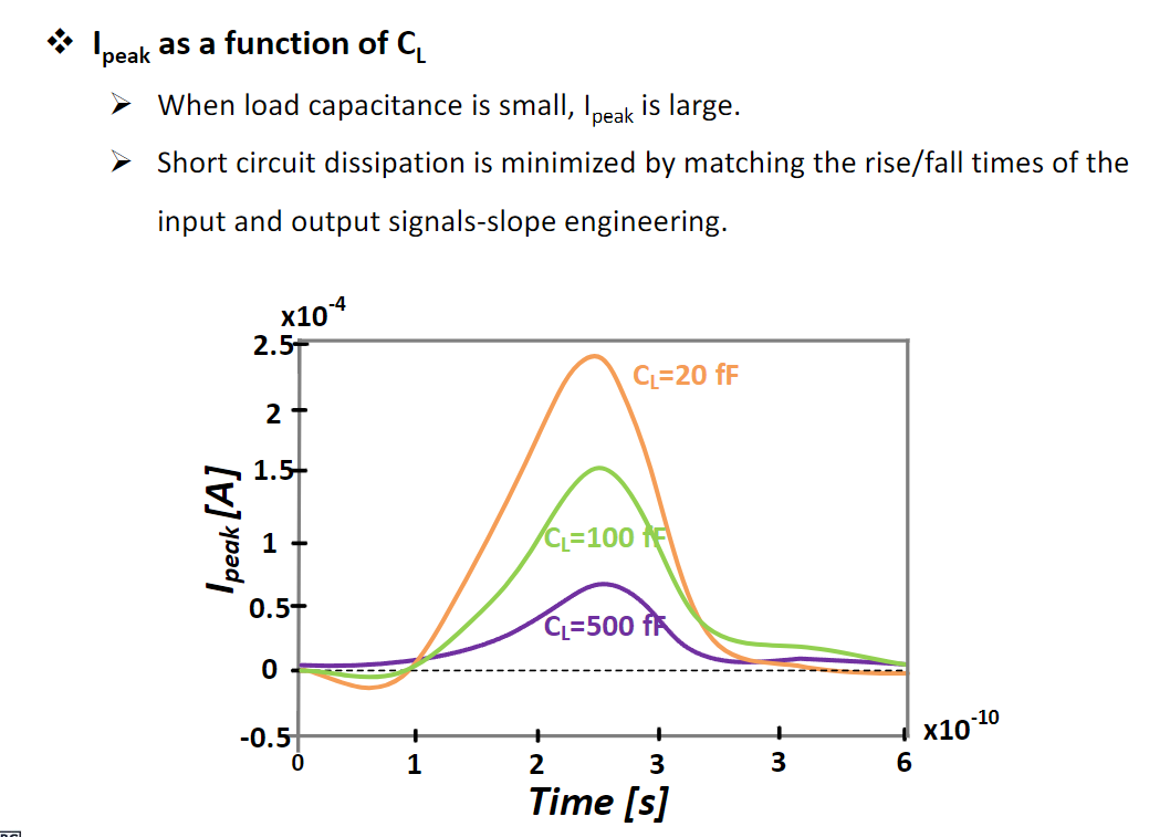
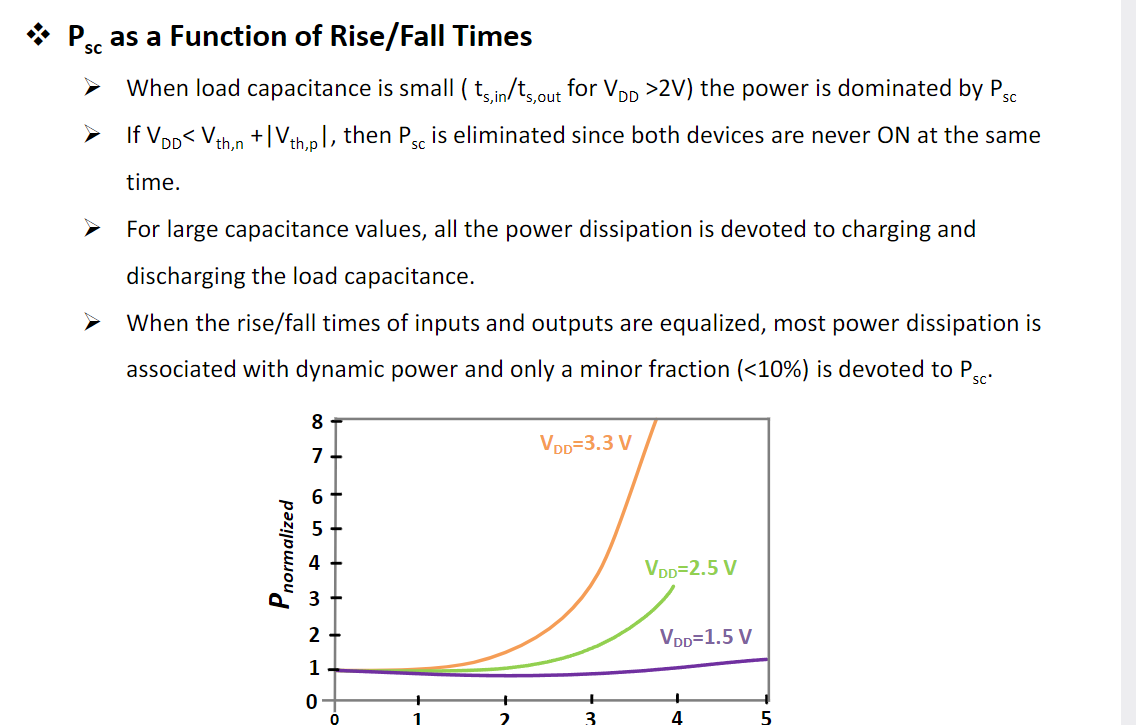
Short-Circuit Power
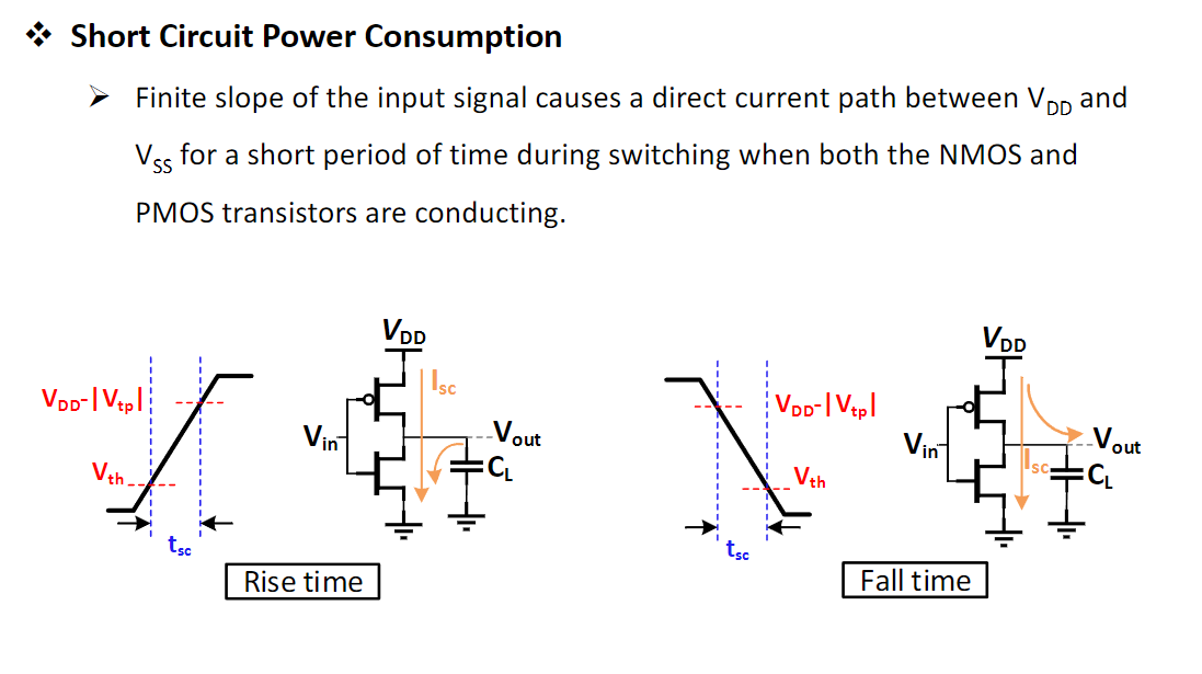
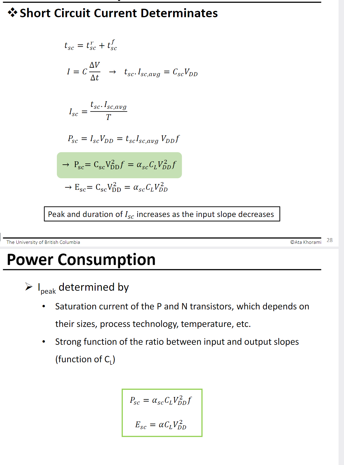
Small load capacitance -> Output fall time substantially smaller than input rise time
Static Power
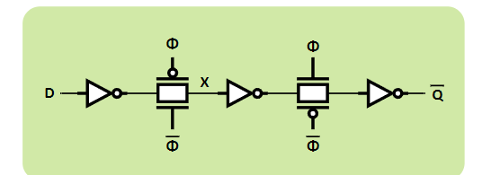
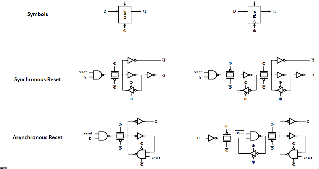
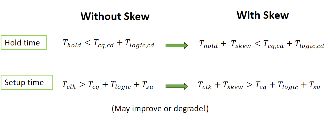
Sequential ciruits
Comments
Loading comments…